 40G/100G Optical Transceivers
 10G/25G Optical Transceivers
 155M/622M/2.5G Optical Transceivers
 100M/1G Optical Transceivers
 FC 16G/32G Optical Transceivers
 CWDM/DWDM Optical Transceivers
 100M/1G/10G Coppers
 Active Cable AOC
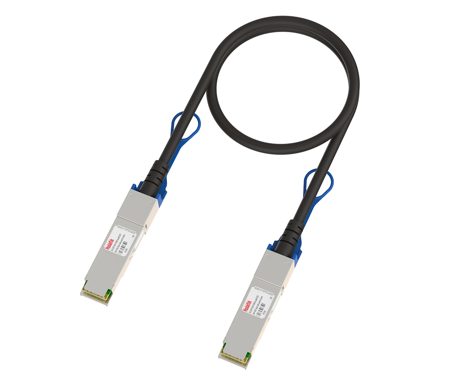 Direct Attach Cable DAC
 Regular/MTP-MPO Fiber Patch Cords
 MT2011
 MT2010
 CodingBox
Chemical Nickel Palladium gold circuit board process
Time: 2019-02-06
Optical module products tend to be small, high-speed, and with the popularity of network communications, optical module demand continues to rise, and the price continues to decline.In order to adapt to the miniaturization and batch production of optical module and reduce the cost,The COB process is to directly fix bare chips, lasers, and other devices to the circuit board, using wire bonding technology, and directly interconnect signals with gold wires through Thermal Ultrasonic Welding Technology.In order to meet the production and requirements of the optical module in COB process, the circuit board needs to meet the following requirements:The circuit board solder pads need to be plated with soft gold (pure gold) in order to integrate with the gold wire for binding. The gold fingers of the circuit board need to have good wear resistance to meet the requirements of insertion and removal. The surface treatment process of the circuit board should not be too complex, resulting in high processing time and cost, and meeting the requirements of ROHS.
There are only two kinds of surface treatment processes that can meet the requirements of such optical module circuit boards:
The first process is the Electroless Nickel Immersion Gold (ENIG) process : plating nickel on copper plate and a layer of soft gold on nickel. Nickel plating is because nickel has good adhesion to both copper and gold. In order to prevent nickel from migrating to the surface through the fine pores of the soft gold coating, which can contaminate and corrode the solder pad and cause binding difficulties, the soft gold layer needs to have a certain thickness, with a gold plating thickness of 0.3um or more. In the gold finger area, the soft gold is not wear-resistant and requires local plating of hard gold (an alloy of gold). The ENIG process still has a difficult problem in production: binding requires a gold plating thickness of over 0.3um, while soldering requires a gold thickness of around 0.05um for good soldering reliability, therefore, it is necessary to adopt different thickness of gold plating in different areas of the circuit board. Thus it can be seen, because the circuit board needs to be processed in the welding area, the binding area and the Gold finger area respectively, the process of the circuit board is complex, the cost is high and the yield is low.
The second process is the Electroless Nickel Electroless Palladium Immersion Gold (ENEPIG) process, also known as the Nickel Palladium Gold process. The earliest surface treatment process developed by Intel was to add a palladium plating layer between nickel plating and pure gold plating, separating the nickel plating from the gold plating layer and isolating the migration of nickel to the surface gold layer,the thickness of the gold plating layer can be reduced to less than 0.1 um.Because wear resistance and higher hardness of metal palladiumcompared to hard gold, and the palladium with thickness of about 0.3 um solves resistance to insertion and removal problem of the gold finger, the entire circuit board adopts a surface treatment process, which shorterns the production cycle and increases the yield ,thereby reducing costs.Both palladium and gold are chemical property metals, and the circuit board has a long storage time and can undergo multiple reflow soldering processing.When the ENEPIG process was first developed, it was difficult to control the cost due to the much higher price of palladium compared to gold. As the price of palladium metal decreased, the current price of palladium is less than half that of gold, it is an inevitable trend for the ENEPIG process to replace the ENIG process.
Table 1 comparison of the characteristics of the two processes
|
characteristics
|
EPIG
|
ENGPIG
|
|
storage time
|
due to nickel migration, short
|
long
|
|
processing procedure
|
multiple gold plating (complex)
|
palladium-plated gold dip (simple)
|
|
surface gold thickness
|
thick (0.3 μm)
|
thin (< 0.1 μm)
|
|
binding functionality
|
Yes
|
Yes
|
|
reflow soldering times
|
unreliable
|
reliable
|
|
gold finger
|
hard gold, wear resistant
|
thick palladium thin gold, wear-resistant
|
|
cost
|
the gold plating layer is thick and the cost is high
|
palladium is cheaper and less costly than gold
|
|
reliability
|
low
|
palladium has thermal diffusivity and high reliability
|
The SFP28-25G SR/AOC, QSFP28-100G SR/AOC and QSFP-40G SR/AOC products of ModuleTek Limited are made by EPENIG process, which has good producibility. Welcome to purchase.
If you have any questions about the above content, you can contact us by Email : web@moduletek.com


