Introduction to COB process for optical modules
Time: 2020-02-23
1. What is COB process
In recent years, high-speed optical modules have often mened the COB (Chip on Board) process. The so-called COB process refers to the process of directly fixing exposed chips onto printed circuit boards, then bonding them with gold wire leads, and then using organic adhesive to package and protect the chips and leads. Compared with conventional processes, this process has high packaging density, simple process, fewer signal integrity issues, and certain advantages in price.
2. Main processes of COB process
The COB process mainly includes three processes: solidification, threading, and coupling.
2.1 Solidification
By using high-precision solid-state instruments, the bare chip is fixed on the surface of the PCB through conductive silver adhesive, as shown in the figure. Firstly, the machine identifies the position where the PCB board needs to be fixed with silver glue, and dips an appropriate amount of silver glue into it through a glue dispensing needle. Then, the machine suction nozzle absorbs the optical chip and the electrical chip from the material box and places them at the position where the silver glue was just fixed. After manually detecting the accuracy of the fixed crystal, the chip can be fixed through high-temperature baking.
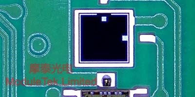
Figure 1 Solidification Diagram
2.2 Wiring
Wiring is the process of connecting electrical and mechanical connections between electrical chips and optical chips, as well as between electrical chips and PCB pads. It is commonly done using a wiring machine. Solidification and wiring are crucial. Wiring needs to meet tensile testing requirements, and there are also certain requirements for the length of the wiring. Long or short wiring can affect actual performance, such as sensitivity, emission eye pattern, and optical module failure analysis.
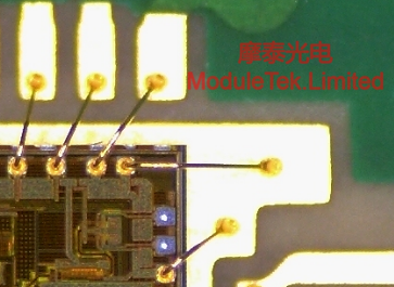
Figure 2 Wiring Diagram
2.3 Coupling
Coupling is the process of fixing the lens on the PCB board, so that the light energy emitted vertically by the VCSEL is reflected and emitted parallel through the lens. The coupling step is crucial, as skewed lenses or unreasonable UV adhesive coating can lead to changes and differences in the emission power and sensitivity.
The general operation process is as follows: after downloading the program for the PCB core with fixed crystal wiring, the adapter lens is coupled to the optimal position for receiving and emitting light through an automatic coupling machine. First fix the lens with UV glue, then cure with black glue, and bake for a few hours in a high-temperature environment to complete. Through COB automatic coupling machine processing, the degree of automation is high, and manual loading and unloading are only required, which can achieve automatic coupling and dispensing, greatly improving the module processing efficiency.
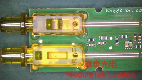
Figure 3 coupling
Moduletek Limited has its own fixed crystal, production line, and automatic coupling production line, which can provide various optical module products based on COB technology. We welcome everyone to choose and purchase.
If you have any questions about the above content, you can contact us by Email : web@moduletek.com

 40G/100G Optical Transceivers
 10G/25G Optical Transceivers
 155M/622M/2.5G Optical Transceivers
 100M/1G Optical Transceivers
 FC 16G/32G Optical Transceivers
 CWDM/DWDM Optical Transceivers
 100M/1G/10G Coppers
 Active Cable AOC
 Direct Attach Cable DAC
 Regular/MTP-MPO Fiber Patch Cords
 MT2011
 MT2010
 CodingBox

